
BIOS POST Codes, diagnostic messages
This chapter is dedicated to reviewing typical error codes and the most common
diagnostic messages generated by POST BIOS, produced by various companies
pany. Although the information offered covers software products,
appeared in different years, the main information parameters of the tests are relevant
and for diagnosing malfunctions of modern computers.
- Introduction to POST Award BIOS Medallion V 6.0 codes
- POST AMI BIOS 8 V1.4 checkpoint codes
- POST Phoenix BIOS V 4.0.6 codes
- Description of diagnostic messages POST Award BIOS V 4.51PG
- Diagnostic error messages POST AMI BIOS 8 V 1.0
- Error codes and diagnostic messages POST Phoenix BIOS V 4.0
Award BIOS Medallion V 6.0
CF Early detection of processor type. Recording results in CMOS. CMOS read/write functional test. If detecting the processor type or writing to CMOS fails, a fatal operation error is set and POST execution is stopped
C0 Chipset pre-initialization. Prohibition of shadow RAM areas, disabling L2 cache.
Clearing the L1 cache
C1 Checking the type, size, high address and ECC of RAM. Checking the first 256 KB of RAM. Organization in this area of a transit buffer, into which from Flash BIOS
Boot Block is copied to verify checksums
0C Checking the BIOS checksum and the presence of the BBSS tag. If the checks are incorrect, a decision is made about partial damage to the Flash BIOS IC. If checks
are correct, the system BIOS unpacking program is copied to the buffer
C3 Unpack system BIOS into RAM, copy optional system into RAM
BIOS. Preparing for BIOS Shadowing
C5 Copy the executable POST code to the shadow RAM area E000h-F000h. Transfer control to the Boot Block module. Start POST from shadow RAM. Checking the integrity of the BIOS structure. If the verification checksums BIOS service fields match, the RAM check continues, otherwise control is transferred to BIOS recovery programs
Performing POST on Shadow RAM
01 At physical address 1000:0000h the BIOS module is unpacked - program XGROUP, which allows you to install all motherboard resources, including system timer, interrupt and DMA controllers, mathematical coprocessor and video controller by default
03 Performing early initialization of Super I/O chip, the first stage was completed on
steps of the algorithm CFh and C0h
05 Setting the initial attributes of the video system. Checking the CMOS status flag, its contents are reset
07 Reset the input and output buffers of the keyboard controller (compatible with IC 8042 or 8742). The controller is part of the Super I/O system chip fees. Self-test, initialization of the keyboard controller. Allowed keyboard interface connection
08 Prohibition of connecting the PS/2 computer mouse interface. The type of keyboard interface is determined (PS/2 or AT/DIN). Programmable keyboard controller. Keyboard allowed
0A The PS/2 mouse interface is still disabled. For some systems - determining the ports to which the PS/2 keyboard is connected and mouse, which may cause port reassignment
0E Test the shadow segment F000h with read and write cycles. This area will be used for DMI and ESCD. If the check is incorrect, then a sound signal is generated and error code EFh is output to port 0080h
EF If the written and read data from segment F000h do not match, an error is detected and the POST execution is stopped
10 Determining the type of installed Flash BIOS. The check allows you to select for
BIOS corresponding writing program with which to boot special command Read Intelligent Identifier. The command is also used procedures for modifying ESCD and DMI blocks that can be overwritten both during loading and after it - when applications access functions Plug and Play or DMI. BIOS code running in a work session will be decoded and rewritten to the Run-time area (F000h). Programming chipset registers
12 Perform a chain of CMOS tests. The RTC clock is set to power mode.
CMOS cells are further used to store intermediate results during the initialization procedure. In particular, cells are loaded default values
14 Perform early chipset initialization. At the first stage, programming resources that are not available to the motherboard designer. At the second stage into registers The chipset is loaded with values changed using the MODBIN utility. Fine-tuning of RAM and PCI devices becomes possible
16 Early initialization of the system clock - setting values according to default
18 Determination of processor parameters: manufacturer company, family, generation, determination of the type and size of L1 and L2 cache, SMI type. Executing the CPUID command function (processor codes and architecture vary from manufacturer to manufacturer). Checking processor registers, measuring processor core clock speed.
After the function is executed, the result is stored in a 128-bit word, formed by the register cells of the central processor - EAX+EBX+ECX+EDX. To decrypt the value of the cache used, code shifted and moved to the AL register
1B Initialization of the interrupt vector table (volume 1,024 bytes, 256 types interrupts). At this stage, the types for 32 vectors (INT 00hINT 1Fh) pointing to BIOS procedures are established. Performing checks to ensure Y2K compliance
1C Checking CMOS checksum and supply voltage compliance
battery nominal. If errors are detected, the values are set according to
defaults set by the motherboard manufacturer
1D On single-processor systems, initial system setup is performed Power Management
1F Loading a keyboard matrix for a laptop from the external XGROUP module.
The matrix is a table of conversions of values entered <Fn> keys
21 Initializing the Hardware Power Management system for laptops. Formation of a table of physical parameters, structure for maintenance Autonomous battery power supply, energy saving functions during operation hard drives, as well as operations to save a RAM image on disk
23 Math coprocessor detection. Checking the number of cylinders - 40 or 80, as well as the type installed floppy disk Perform early chipset initialization.
Preparing a BIOS resource map intended for further installation
Plug and Play devices, as well as airborne devices on the PCI bus
24 Processors of the Intel P6 and P7 generations provide the ability to organize
access to microprogram memory, which contains execution algorithms each machine command. At this stage, the firmware microcode may changes may be made to modernize algorithms or introduce new microcodes designed for new machine instructions. Procedure Microcode updates are performed as follows.
• Using the CPUID command, the processor is identified and its parameters - type (Type), family (Family), model (Model) and coefficient
frequency multiplication (Stepping).
• From the microcode update module stored in the BIOS, the required
the block has a capacity of 2,048 bytes and is unpacked not into RAM, but into SM RAM.
• The processor microcode is updated. Some Intel processors require additional identification. The resource distribution map is being updated. Plug and Play devices are initialized. Information about resources, requested by Plug and Play devices, is updated based on scanning data from CMOS, BIOS extensions located on buses
airborne extensions, as well as information stored in the ESCD data block.
Writing data to ESCD is deferred until the final stage of POST execution
25 Early PCI initialization. Enumeration of devices on the bus. Purpose
RAM and airwave resources.
Search for video system device, BIOS extensions and write information to
area C000:0h (segment address in the CS register:offset address in the IP register)
26 Configuring the logic that serves the Vendor Identification lines. Completes system clock initialization. Shutdown synchronization of unused DIMM and PCI slots.
Initialization of the voltage and temperature monitoring system performed
according to motherboard type
27 Interrupt enable INT 09h. Reinitializing the Controller keyboard based on new data (interrupt vector tables, chipset initialization). For BIOS, a 16-character input buffer is created and the area is set memory for full functioning
29 Programming MTRR registers of the P6 generation processor, as well as Initialization of the APIC controller of Pentium processors. Programming the chipset (such as an IDE controller) according to with settings in CMOS. Measuring the internal processor frequency. Calling the video system BIOS extension
2D Initialization of the multilingual module. Sending data to be displayed on the display screen (Award screen saver, type processor and its speed)
33 Super I/O Chip Programming
3E Check the interrupt controller channel 1 masking bits (compatible with IC 8259)
40 Check the masking bits of interrupt controller channel 2 (compatible with IC 8259)
43 Checking the functioning of the interrupt controller (compatible with IC 8259)
49 Calculate total memory by checking each double word in each 64 KB page.
Recording a program designed to test AMD family processors
4E Programming MTRR registers of the Syrix family processor. Initialization
L2 cache of P6 generation processors, as well as APIC initialization for P6
50 USB bus initialization
52 Check all memory, clear extended memory
55 For a multiprocessor platform, the number is displayed processors
57 Displays the Plug and Play logo screen. Early provisioning of Plug and Play devices
59 Activating the anti-virus protection resource - integrated anti-virus Trend Anti-Virus products
5B Optional message display function for floppy input BIOS update utilities - AWDFLASH.EXE
5D Connecting integrated modules - Super I/O and audio system
60 Stage allowing you to load the Setup program.
Before this POST stage you must have time to press the appropriate key
65 Initializing a PS/2 computer mouse
67 Preparing information for the address space intended for call functions: INT 15h (register contents AX=E820h)
At this stage, scan codes are received from the keyboard and processed by the 8742 controller and the processor are impossible, since interrupts are prohibited, the area is not prepared BIOS data and the keyboard is not initialized. Setup BIOS settings should not contradict execution of POST sequence
69 Enabling L2 cache
6B Programming chipset registers in accordance with the elements described in Setup and in the autoconfiguration table
6D Resource assignment for all Plug and Play devices. Automatic COM port allocation for integrated devices if the Setup option is set to “AUTO”
6F Initialize the floppy disk controller. Additional configuration of floppy disk registers
73 Optional BIOS update utility input function AWDFLASH.EXE if
it is located on the floppy disk and the key combination <Alt+F2> is selected
75 Detection and installation of all IDE devices: hard drives, LS-120, ZIP, CD-R/RW, DVD, etc.
77 Serial and Parallel Port Detection
7A Detecting and installing a math coprocessor
7F Switch to text mode.
82 Depending on the type of chipset and motherboard, an area is allocated in RAM for
power management. The ESCD table is updated with the latest management-related changes food. After removing the splash screen with the EPA logo, the video mode is restored. Request a password, if provided by CMOS settings
83 Restoring data from a temporary storage stack in CMOS
84 Displays the message “Initializing Plug and Play Cards...” about detected
Previously Plug and Play devices and settings
85 USB initialization completed. Determining boot order from SCSI hard drives
87 Switching the video system to text mode. Building SYSID tables in the DNI area according to the “System” specification Management BIOS"
89 If the Setup program allows the use of the ACPI protocol, the top 4 GB address space area, corresponding tables are inserted
8B Scan in PCI space for BIOS extensions intended for
implementation of the AOL (Alert On LAN) protocol. Initializing AOL Tools
8D Allows the use of non-masked support logic NMI interrupts. Enable the use of RAM module parity
8F For PS/2 mouse hot plugging, IRQ line 12 is enabled. IRQ 11 line maintenance, normalization of line noise parameters interrupt requests
91 Preparing conditions for servicing hard drives in Power mode Management. Operations of this type (Suspend to RAM) can be implemented in a working operating system session. Setting BIOS variables that store base addresses of serial
and parallel ports that have BIOS expansion programs
93 Preparing to save information about boot device partitions
94 If Setup is provided, the L2 cache is enabled. The Boot Up Speed parameter is programmed. Completing initialization of the chipset and power management system.
Removing the BIOS startup splash screen, a table is displayed on the monitor screen
resource distribution. Configuring registers for AMD K6 family processors.
The final update of the registers of the Intel P6 family of processors.
Final initialization of the Remote Pre Boot subsystem
95 Setting the automatic transition to winter/summer time Daylight Saving.
Programming the Keypad Controller for Keystrokes per Second and Time waiting before entering auto-repeat mode. Reading keyboard KBD ID. For a 101-key keyboard, the NumLock flag is set according to with CMOS information
96 Saving information about boot device partitions. On multiprocessor systems, the final system configuration is performed, service tables and fields used in the work session are formed operating system. Configuring registers for Cyrix family processors.
Diagnosing faults when starting a PC
FF Save boot device partitions for later use integrated anti-virus tools Trend Anti-Virus
and Paragon Anti-Virus Protection. Enable the use of L1 cache. A sound signal for the end of POST is generated on the system unit speaker. Building and saving the MSIRQ table. Preparing to boot the operating system
FF Transfer control to the initial sector loader program BOOT.
Performing BIOS INT 19h interrupt.
The called routine allows (according to the BIOS Features menu option)
Set Up program) poll boot devices to search for a sector
downloads. To load information from the sector Cylinder: 0, Head: 0, Sector:
1 is read at address 07C0:0000h, after which control by the FAR JMP command
sent to the beginning of this block
NOTE.
ECC (Error Correcting Code) - error correction code is used in RAM modules, helping
increasing PC fault tolerance. ECC allows you to correct a single bit error
and detect in two digits. Therefore, a computer whose memory uses such
codes, in case of an error in one bit can work without interruption, and the data is not
will be distorted.
BBSS (Boot Block Specification Signature) - boot block specification signature label.
SMI (System Management Interrupt) - hardware integrated into the processor,
designed to control power consumption. To service these
components uses a high priority interrupt.
Y2K - requirements for commercial computer system products for
ensuring interoperability, functionality and other parameters that have
place before and after 2000.
DMI (Desktop Management Interface) is a protocol that allows interaction
software with motherboard components.
MTRR (Memory Type Range Registers) - registers of processors of the P6 and P7 generations, into which
Data is entered that describes the properties of memory areas and determines the type of memory caching.
APIC (Advanced Programmable Interruption Controller) - advanced programmable
interrupt controller included in the chipset. P6 generation processor also
has a similar controller for multiprocessor applications.
MSIRQ (Microsoft IRQ Routing Map) - interrupt distribution map table,
standardized by Microsoft.
SM RAM (System Management RAM) is one of the names for random access register memory
small capacity provided in the processor architecture, starting with Pentium Pro
and higher, intended for storing service data.
POST BIOS codes and diagnostic messages from various companies
System Events codes
B0 Exception error in Protected Mode processor operation mode
B1 NMI request recognition error
B2 NMI execution error
Code activated when servicing APM or ACPI components
55 Energy saving with +12 V power supply cut-off
66 Switch to operating mode with minimal power consumption
D0 Interrupt to exit power saving mode by event
D1 Switching the processor into power saving mode by reducing its clock speed frequencies
D2 Switch to partial power saving mode using ACPI technology
D3 Using the SMI component to enter power saving mode
D7 Switching the processor into power saving mode using APM technology
D8 System transition to power saving mode using APM technology
D9 Putting the system into full power saving mode
Message about fatal operations errors
EC ECC code processing error
ED Hard drive error when returning from power saving mode
EF Data mismatch when writing to and reading from segment F000h
POST AMI BIOS 8 V1.4 checkpoint codes
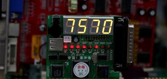
Diagnostic tools are used to display POST AMI BIOS checkpoints. boards
POST Diagnostic Card, indicators on motherboards, and control displays
AMI BIOS Checkpoint Display. The display is a line of code in the lower right corner of the monitor screen, displaying pressed during POST

2Ah initialization of devices on the system bus.
38h initialization of IPL devices.
39h indication of errors during bus initialization.
95h initialization of buses controlled by BIOS extensions.
DEh - RAM configuration error.
DFh - RAM configuration error.
[0000] initialization of all devices on the buses of interest is prohibited.
[0001] initialization of static devices on the buses of interest.
[0010] initialization of information output devices on the buses of interest.
[0011] initialization of information input devices on the buses of interest.
[0100] initializing system load (IPL) devices on the buses of interest.
[0101] initialization of general purpose devices on the buses of interest.
[0110] error message for the tires of interest.
[0111] initialization of devices controlled by BIOS extensions (for all buses).
[1000] initializing BIOS boot extensions corresponding to BIOS Boot
[0000] system initialization procedures (DIM).
[0001] buses for connecting integrated system devices.
[0010] ISA bus.
[0011] EISA bus.
[0100] ISA bus Plug and Play.
[0101] PCI bus.
[0110] PCMCIA bus.
[0111] MCA bus
If a RAM configuration error is detected, you can use the diagnostic port to there is a cyclic sequence of codes DEh, DFh and configuration checkpoints tions that can take the following values.
00 No RAM detected.
01 Various types of DIMMs are installed.
02 reading from the SPD (Serial Presence Detect) node of the DIMM failed.
03 The DIMM cannot be used at this frequency.
04 The DIMM cannot be used on this system.
05 error in the low memory page.
Diagnosing faults when starting a PC
D0 Switch to flat address space display mode, limited to 4 GB, and signal resolution GA20 (Gate A20). Examination boot block checksum
D2 Disables the cache and then performs a test to determine the size of the entire memory
D3 If the size of the entire memory has not yet been determined, then the DRAM is regenerated, after whereby the amount of RAM is determined by the Bootblock code. Cache restarts and the chipset is additionally initialized
D4 The 512 KB base memory is tested, the first 8 MB of cache is configured,
stack is installed
D5 Bootblock codes are copied from Flash BIOS to the lower RAM address area.
Shadowed BIOS programs now run from system memory
D6 Performs key sequence test and OEM specific test to check the integrity of information in Flash BIOS. Checking the BIOS checksum. If a BIOS recovery is required,
then the checkpoint code E0h is generated
D7 CPUID values are written to the processor register file. The Bootblock Runtime interface module is sent to RAM and passed control
D8 The Runtime module is unpacked into RAM. CPUID information is transferred to storage in RAM
D9 The system BIOS is unpacked and copied into RAM. All BIOS information remains in the shaded address area. space up to 1 MB (E000h-F000h)
DA CPUID values are written back to the processor registers for storage.
Loading control is transferred to the POST execution kernel - (Execute POST Kernel)
E9 Setting up floppy disk controller registers and writing data. Trying to read from floppy disk
EA Preparing ATAPI hardware for operation. Trying reading from ATAPI CD-ROM and disk memory
EB If the operation of ATAPI hardware is prohibited, then switch to control point E9h
EF If errors are read from the media, then go to checkpoint EBh
F0 Search the root directory for a predefined file name recovery
F1 Recovery file not found
F2 Start reading the FAT table and analyzing its contents to find clusters,
busy with recovery file
F3 Start reading cluster by cluster recovery file
F5 Disable L1 cache
FA Verifying the validity of the recovery file configuration by comparison with current configuration from Flash BIOS
FB Preparing the chipset and OEM specific tools for writing to Flash BIOS.
Detection of the corresponding partition in Flash BIOS. Confirmation that that the size of the detected partition is equivalent to the size recoverable file
F4 The size of the detected partition is not equivalent to the size of the file being restored
FC Cleaning Flash BIOS partition
FD Programming Flash BIOS partition
FF Flash BIOS has been properly updated. Recording is prohibited Flash ROM.
ATAPI hardware is disabled. The register is reset to the CPUID value.
Control is transferred to the Flash BIOS area from F000h to F000:FFF0h
POST AMI BIOS 8 V 1.4
03 Operations prohibited: parity, NMI interrupt handling, startup of the video system and the operation of the DDP controller is blocked.
The data area of the current BIOS execution and POST is initialized
04 The battery voltage and control voltage are being checked CMOS amounts.
If the checksum is not correct, the power-on memory is updated with the default value and the password is cleared. Status register A is initialized. The variable database for Setup as well as both is initialized interrupt controllers (compatible with IC 8259)
05 Interrupt request lines IRQ controllers are initialized
interrupts from airborne devices, and also a table of interrupt vectors is marked
06 The interval timer is being read/written and the interrupt handler POST INT 1Ch.
Enable line IRQ 0
08 The processor is initializing. The BAT test of the keyboard controller is performed, synchronization is enabled keyboards
C0 Preparing the processor for operation. Disabling the cache, preparing the processor controller for operation APIC controller
C1 Initial setting of processor parameters for downloading information
C2 Initial setup of processor parameters for performing POST
C5 Enumeration and initial configuration of processor applications
C6 Restarts cache for initial processor setup
C7 Processor exits initialization mode
0A Initializes keyboard controller (8742 compatible)
0B Detects a connected PS/2 computer mouse
0C Detection of connected keyboard
0E Various input devices are checked and initialized. Modification of the variable kernel.
Interrupt capture INT 09h. The handler prepares the IRQ 1 line. Unpacking all available language modules, displaying the BIOS logo and the Silent modules logo
13 Early initialization of chipset registers
24 Unpacking and initializing BIOS modules of any platforms
30 The SMI (System Management Interrupt) component is initializing
2A Various devices are initialized via DIM (Device Initialization Manager)
2C Various airwaves are initialized. Detects and initializes the connected video adapter that contains BIOS extension
2E All output devices are initialized
31 Allocating a memory area for the ADM block and unpacking it. ADM initialization and control transfer. Setting the language and font. Activating the ADM module
33 Loader module applications are initializing. Preparing the display window for viewing text information
37 Screensavers for messages, processor information, and installation keys and other OEM specific information (manufacturer)
38 DIM component is initializing
39 DMA controller is initializing
3A Date/time in RTC is initialized
3B Checking all memory mounted on the system board. Test case for the <Del> and <Esc> keys intended for reducing the number of memory test passes.
Displaying the amount of shared memory on the system board
3C Continue initialization of chipset registers
40 Detection of parallel devices successfully installed in the system and serial ports, mathematical coprocessor, etc. Modification of BDA, EBDA, etc.
50 Programming memory control modules of various types, presented in the system, adjusting the amount of RAM
52 Modification of RAM volume in CMOS. Placement in EBDA RAM
60 The state of the <Num Lock> key is initialized and programmed keyboard typing speed
75 Interrupt INT 13h is initialized and prepared to search for IPL devices
78 BIOS management of IPL devices and BIOS extensions is initializing
7A The remaining BIOS extensions are initializing
7C Generating and writing ESCD contents to non-volatile memory
84 Reporting errors encountered during POST
85 Display errors on the monitor for the user, receive a response from user to the information provided
87 If you want to set up your PC and called the Setup BIOS program, it should start
8C Completing initialization of chipset registers
8D If the ACPI subsystem is supported, the ACPI table is built
8E Programming parameters of peripheral devices. Disable or enable NMI interrupt (depending on setting)
90 Final POST initialization of SMI module
A0 Boot password is checked (depending on setting)
A1 The cleaning operation required before starting the program is in progress operating system boot
A2 Preparing the screen display of the executable BIOS modules involved in loading the operating system. Filling free memory in the address space of the segment from F000h to 0FFh. Initializing the Microsoft IRQ Routing Table. Preparing the language module to be used when loading. Prevent display of system configuration (depending on setting)
A4 The language module is initializing
A7 If the appropriate option is selected, the splash screen will be displayed system configuration. Pre-boot processor setup, which also includes seeding MTRR registers
A8 Completing MTRR programming, preparing processor for boot operating system
A9 Waiting for user input of configuration data (depending on settings)
AA Reset POST interrupts - INT 1Ch, INT 09h. Disabling the ADM Module
AB Preparing the BBS to load the INT 19h interrupt handler
AC Complete initialization of chipset registers
B1 Saving context for the ACPI subsystem
00 Transfer of control via interrupt INT 19h to the operating system loader
Phoenix BIOS V 4.0.6
02 Checking whether the real operating mode of the central processor is enabled
03 Disable non-maskable NMI interrupt
04 Determination of processor type
06 System hardware is initializing
07 Disable shading and execute BIOS code
08 Early chipset initialization
09 Setting the IN POST flag
0A Initialize processor registers
0B CPU cache resolution
0C Early cache initialization
0E Airborne components are initializing
0F Initializing IDE
10 The energy saving system (Power Management) is initialized
11 Working registers are loaded with POST initial values
12 Restoring the processor control word during a “warm start”
13 PCI BUS Mastering devices are initialized
14 Keyboard controller is initializing
16/1-2-2-3 The Flash BIOS checksum is checked (if an error is detected, then a sequence of beep error codes is generated)
17 The cache is initialized before automatically detecting the amount of RAM
18 Interval timer is initialized (8254 compatible)
1A DMA controllers are initialized (compatible with IC 8237)
1C Resetting interrupt controllers
20/1-3-1-1 DRAM RAM regeneration test is performed (if an error is detected, then
a sequence of beep error codes is generated)
22/1-3-1-3 The keyboard controller test (compatible with IC 8742) is performed (if
an error is detected, a sequence of error codes is generated)
24 Setting the ES segment register to 4 GB
28 The amount of RAM is determined
29 Launching the RAM maintenance program (POST Memory Manager)
2A Clear 512 KB base RAM area
2C/1-3-4-1 The 512 KB RAM address lines are being tested. If a RAM error is detected on the address bus (xxxx), then a sequence of beep error codes.
Faulty bits are counted starting from zero, for example, code 2C 1020 means
bit failure 0001 0000 0010 0000, i.e. twelfth and fifth grades
2E/1-3-4-3 The 512 KB RAM data lines are being tested. If an error is detected on the RAM data bus (xxxx), then a sequence of beep error codes
2F BIOS information is obscured. Allow cache
30/1-4-1-1 512 KB base memory RAM data bus error in bit xxxx high byte
32 Determining the processor clock speed
33 Running Phoenix Dispatch Manager
36 Shutdown during “warm start”
38 BIOS information is obscured
3A Determining cache size
3C Continued configuration of chipset registers
3D Continue loading free registers with POST values
41 Additional memory is initializing to load the ROM Pilot program
42 Interrupt vectors are initialized
45 Non-Plug and Play devices are initializing
46/2-1-2-3 Copyright is checked (if a discrepancy is found, then
a sequence of sound codes is generated)
47 I20 technology components are initializing
48 Uploading video system configuration data from CMOS
49 PCI bus and devices are initializing
4A All video adapters in the system are initialized
4B Run QuietBoot (Optional)
4C BIOS video extension is obscured
4E The BIOS copyright message appears on the splash screen
4F Loading the MultiBoot utility
50 The screen displays the processor type and clock speed
51 EISA bus components are initializing
52 Keyboard test
54 Keystroke (if required)
55 USB devices allowed
58/2-2-3-1 Unexpected interrupt test (a sequence of beep codes is generated)
59 POST message rendering facilities are initializing
5A Displaying the “Press F2 to enter SETUP” prompt on the screen
5B Disabling the processor cache
5C Checking the RAM memory area between 512 and 640 KB
60 Checking additional memory
62 Checking additional memory address lines
64 Maintenance Patch (UserPatch 1)
66 Continued configuration of cache registers
67 APIC module registers are initialized in a multiprocessor system
68 Enable external and internal caches
69 Setting the memory area for loading the SMM (System Management Mode) program
6A Display external L2 cache size
6B Load special modes and default settings (optional)
6C Display information about the shadow area of RAM on the screen
6E Displays information about the upper RAM memory on the screen for possible
recovery of the UMB (Upper Memory Block) block
70 Displaying Error Messages on the Screen
72 Running a sample test to identify configuration errors
76 Running a sample test to detect keyboard errors
7C Setting hardware interrupt vectors
7D The Intelligent System Monitoring subsystem is initializing
7E Math coprocessor is initializing
80 Prohibition of integrated Super I/O ports and IRQ lines
81 Final initialization of devices
82 Detecting and Configuring External Serial Ports
83 IDE controllers are initializing
84 Detecting and configuring external parallel ports
85 IBM PC clone Plug and Play devices are initializing
86 Re-initialization of integrated airborne ports
87 Executing MCD (Motherboard Configurable Device) Program (Optional)
88 BIOS database memory area is initializing
89 NMI non-maskable interrupt enabled
8A Additional BIOS database memory area is initializing
8B The PS/2 computer mouse is checked and initialized
8C The floppy disk controller is initializing
8F Count the number of ATA devices (optional)
90 Hard disk controllers are initializing
91 Hard disk controllers on the local bus are initializing
92 Maintenance checkpoint transition (UserPatch 2)
93 Building the MPTABLE table for multiprocessor systems
95 Selecting the boot CD-ROM maintenance procedure
96 Clear ES segment register
97 Binding addresses of the table of multiprocessor systems
98/1-2 Search for BIOS extensions. If an incorrect checksum is detected,
then a sequence of sound error codes is generated
99 Executing a program for SMART devices (optional)
9A BIOS extension information is obscured
9C Setting up the energy saving system (Power Management)
9D System security mechanism is initializing (optional)
9E Hardware interrupts enabled
9F Determining the number of ATA and SCSI devices
A0 Set time of day from RTC
A2 Key lock test running
A4 Enter print speed parameters
A8 Clearing the <F2> key call register
AA Scanning the keyboard by pressing the <F2> key
AC Call and start the Setup program
AE Boot flag cleared
B0 Execute troubleshooting example
B1 Receiving notification from RomPilot about the end of POST
B2 POST checks completed, preparing to boot into OR systems
B4/1 If the POST completes correctly, one short beep
B5 QuitBoot (optional)
B6 Password test running (optional)
B7 BIOS ACPI system is initializing
B9 Preparing to execute the boot block search program
BA SMBIOS program running
BB BIOS Plug and Play extensions are initializing
BC Clear parity devices
BD The MultiBoot utility menu is displayed on the screen
BE Clear screen (optional)
BF Reminder about antivirus protection and data backup
C0 Attempt to boot using interrupt INT 19h
C1 Call to execute the PEM program (POST Error Manager)
C2 Error logging facilities are initializing
C3 The means of calling functions for displaying errors on the screen are initialized
monitor
C4 System error handler is initialized
C5 CMOS Plug and Play Check (Optional)
C6 Initializes the note dock module (optional)
C7 Final initialization of the note dock module
C8 Perform additional tests to identify faults (optional)
C9 Additional checksum definition (optional)
CA Interrupt redirection INT 15h to prepare for remote operation keyboards
CB Forwarding the INT 13h interrupt intended for memory devices ROM, RAM, PCMCIA, and disk memory
CC Interrupt redirection INT 10h for serial video preparation (SDVS service)
CD Preparing I/O Address Space and Memory for PCMCIA
CE Digital signature input and message display are initialized on the monitor screen
D0 Response to an exceptional event (Exception Error)
D2 Response to unknown interrupt
D4 Interrupt request procedure violation
D6 Error when exiting protected mode of processor operation with generation of software reset signals
D7 Lack of allocated memory in the Video RAM area to store the current video adapter information
D8 Error generating processor software reset signals
DA Loss of control failure when starting real processor mode
DC Error when exiting protected mode of processor operation with
generation of software reset signals without reinitialization interrupt controller
DD Extended RAM Area Test Error
DE Keyboard controller test error
DF Gate A20 control line selection error
E0 Chipset initialization
E1 Bridge initialization
E2 Processor initialization
E3 Initialize interval timer
E4 Airborne initialization
E5 Perform boot block recovery check
E6 BIOS checksum verification
E7 Jump to execute BIOS programs
E8 Setting the Huge Segment
E9 Executing a Multi Processor program
EA Initialize special manufacturer code (OEM code)
EB Initialization of interrupt controllers and direct memory access
EC Finding out the RAM type
ED Finding out the amount of RAM
EE Executing BIOS Boot Block Shading Program
EF Check RAM
F0 Initialize interrupt vectors
F1 Execute Run Time Clock program
F2 Initialize the video adapter
F3 Execute SMM program
F4/1 One short beep is generated
F5 Clear Huge Segment memory segment
Paulo (Friday, 01 August 2025 18:46)
incrivel