
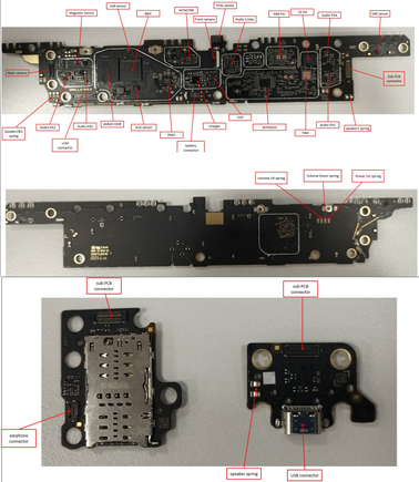
Samsung Galaxy Tab Schematic Diagram, PCB Layout

Samsung Galaxy Tab, Galaxy View, Note, Galaxy Book Schemetic Circuit Digram
PCB Layout. Repair Instruction, Service Manuals Free Download
| Samsung Galaxy Tab A 8.0 SM-P355 Schematic Diagram | Download |
| Samsung Galaxy Tab A7 LTE (SM-T505) schematic Diagram | Download |
| Samsung Galaxy Tab 3 Lite SM-T110 schematic Diagram | Download |
| Samsung Galaxy Tab S2 SM-T715Y schematic Diagram | Download |
| Samsung Galaxy Tab A 9.7 SM-T555 schematic Diagram | Download |
| Samsung Galaxy Tab4 SM-T530 schematic Diagram | Download |
| Samsung Galaxy Tab Pro SM-T525 schematic Diagram | Download |
| Samsung Galaxy Note SM-P605 schematic Diagram | Download |
| Samsung Galaxy Tab A SM-P585 schematic Diagram | Download |
| Samsung Galaxy Tab A 8.0 SM-P350 schematic Diagram | Download |
| Samsung Galaxy Tab A 10.1 SM-P580 schematic Diagram | Download |
| Samsung Galaxy Note pro 12.2 SM-P905 schematic Diagram | Download |
| Samsung Galaxy Tab A / SM-P550 schematic Diagram | Download |
| Samsung Galaxy Note 10.1 SM-P600 schematic Diagram | Download |
| Samsung Galaxy Tab Pro 8.4 SM-T321 schematic Diagram | Download |
| Samsung Galaxy Tab A 10.1 SM-T585 schematic Diagram | Download |
| Samsung Galaxy Tab S2 8.0 SM-T710 schematic Diagram | Download |
| Samsung Galaxy Tab 3 SM-T210 schematic Diagram | Download |
| Samsung Galaxy Tab Pro 12.2 SM-T900 schematic diagram | Download |
| Samsung Galaxy Tab A 8.0 SM-T295 schematic diagram | Download |
| Samsung Galaxy Tab E SM-T567 schematic diagram | Download |
| Samsung Galaxy View SM-T677 schematic diagram | Download |
| Samsung Galaxy Tab 4 7.0 SM-T239 schematic diagram | Download |
| Samsung Galaxy Tab Pro SM-T320 schematic diagram | Download |
| Samsung Galaxy View SM-T670 schematic diagram | Download |
| Samsung Galaxy Tab E 8.0 SM-T377 schematic diagram | Download |
| Samsung Galaxy Tab S4 SM-T830 schematic diagram | Download |
| Samsung Galaxy Tab S2 SM-T719Y schematic diagram | Download |
| Samsung Galaxy Tab A 10.1 SM-T587 schematic diagram | Download |
| Samsung Galaxy Tab S6 SM-T865 schematic diagram | Download |
| Samsung Galaxy Tab S2 SM-T818 schematic diagram | Download |
| Samsung Galaxy Tab S2 9.7 SM-T819Y schematic diagram | Download |
| Samsung Galaxy Book 10.6 SM-W627 schematic diagram | Download |
| Samsung Galaxy Tab E SM-T561 schematic diagram | Download |
| Samsung Galaxy Tab A SM-T385 schematic diagram | Download |
| Samsung Galaxy Tab E SM-T560 schematic diagram | Download |
| Samsung Galaxy Tab 4 SM-T330 schematic diagram | Download |
The main reasons for tablet board failure
Careless handling of the tablet is a fairly general formulation. Particular reasons for the malfunction of the motherboard of a Samsung tablet include the following factors:
- short circuits that damage conductive paths and elements of the power circuit;
- formation of an oxide film after contact with water;
- mechanical failure of the PCB from which the motherboard is made;
- failure of several chipsets as a result of overheating or flooding;
- faulty processor socket on the motherboard.
When you need to change the motherboard of a Samsung tablet, keep in mind that this is a painstaking procedure, the implementation of which requires a certain level of computer literacy. Therefore, independent attempts to repair a faulty device lead to problems on a larger scale and, accordingly, an increase in the cost of repairs. Therefore, in order to avoid mistakes, many users decide to seek help from specialists at a service center when the tablet does not work.
lalala (Monday, 23 June 2025 18:02)
anyone have sm-t820 (galaxy tab s3) ?
Xavier (Monday, 23 June 2025 15:10)
Hello
Do to have information regarding SAMSUNG Galaxy Tab Active 3 & 4 (SM-T570 & SM-T630)?
Hamaty (Saturday, 21 June 2025 23:52)
Samsung Galaxy Tab SM_T970
A52 (Tuesday, 20 May 2025 18:36)
.
Klajdi (Thursday, 24 April 2025 13:41)
ok
Klajdi (Thursday, 24 April 2025 13:28)
flm
iArt (Monday, 10 February 2025 11:18)
tab s6lite (sm-p615) Pls.
ardian (Saturday, 11 January 2025 12:07)
ijin download skematiknya mas
luis (Wednesday, 06 November 2024 01:02)
Muy Buena Pagina. Gracias